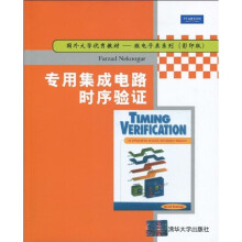
国外大学优秀教材·专用集成电路时序验证:微电子类系列(影印版)

List of Figures
List of Tables
Preface
Acknowledgments
1 Introduction to Timing Verification
1.1 Introduction
1.2 Overview of Timing Verification
1.2.1 Intrinsic vs. Extrinsic Delay
1.2.2 Path Delay
1.3 Interface Timing Analysis
2 Elements of Timing Verification
2.1 Introduction
2.2 Clock Definitions
2.2.1 Gated Clocks
2.2.2 Clock Skews and Multiple Clock Groups
2.2.3 Multifrequency Clocks
2.2.4 Multiphase Clocks
2.3 More on STA
2.3.1 False Paths
2.3.2 Multicycle Path Analysis
2.3.3 Timing Specifications
2.3.4 Timing Checks
2.4 Timing Analysis of Phase-Locked Loops
2.4.1 PLL Basics
2.4.2 PLL Ideal Behavior
2.4.3 PLL Errors
3 Timing in ASICs
3.1 Introduction
3.2 Prelayout Timing
3.2.1 RTL vs. Gate-Level Timing
3.2.2 Timing in RTL Code
3.2.3 Delay with a Continuous Assignment Statement
3.2.4 Delay in a Process Statement
3.2.6 Intra-Assignment Delays
3.2.6 The Verilog Specify Block
3.2.7 Timing in-Gate Level Code
3.2.8 Synthesis and Timing Constraints
3.2.9 Design Rule Constraints
3.2.10 Optimization ConstrAints
3.2.11 Gate and Wire-Load Models
3.2.12 The Synthesis Flow
3.2.13 Synthesis Tips
3.2.14 Back Annotation to Gate-Level RTL
3.3 Post. layout Timing
3.3.1 Man-A1 Line-Propagation Delay Calculations
3.3.2 Signal-Line Capacitance Calculation
3.3.3 Signal Line Resistance Calculation
3.3.4 Signal Trace RC Delay Evaluation
3.4 ASIC Sign-Off Checklist
3.4.1 Library Development
3.4.2 Functional Specification
3.4.3 RTL Coding
3.4.4 Simulations of RTL
3.4.5 Logic Synthesis
3.4.6 Test Insertion and ATPG
3.4.7 Postsynthesis Gate-Level Simulation or Static Timing Analysis
3.4.8 Floorplsnning
3.4.9 Place and Route
3.4.10 Final Verification of the Extracted Netlist
3.4.11 Mask Generation and Fabrication
3.4.12 Testing
4 ProgrAmmable Logic Based Design
4.1 Introduction
4.2 Programmable Logic Structures
4.2.1 Logic Block
4.2.2 Input/Output Block
4.2.3 Routing Facilities
4.3 Design Flow
4.4 Timing Parameters
4.4.1 Timing Derating Factors
4.4.2 Grading Programmable Logic Devices by Speed
4.4.3 Beet-Case Delay Values
4.5 Timing Analysis
4.5.1 Actel ACT FPGA Fsmily
4.5.2 Actel ACT 3 Architecture
4.5.3 Actel ACT 3 Timing Model
4.5.4 Altera FLEX 8000
4.5.5 Altera FLEX 8000 Architecture
4.5.6 Altera FLEX 8000 Timing Model
4.5.7 Xilinx XC3000/XC4000 FPGA Families
4.5.8 Xilinx XC9500 CPLD
4.5.9 Xilinx XC9500 CPLD Architecture
4.5.10 Xilinx XC9500 CPLD Timing Model
4.6 HDL Synthesis
4.7 Software Development Systems
4.7.1 Timing Constraints
4.7.2 Operating Conditions
4.7.3 Static Timing Analysis
4.7.4 Vendor-Specific Timing-Verification Tools
4.7.5 Actel Designer
4.7.6 Altera MAX+PLUS II
4.7.7 Xilinx XACT/M1
A PrimeTime
B Pearl
C TimingDesigner
D Transistor-Level Timing Verification
References
Index
About the Author
内库加(Farzad Nekoogar) is Director of Design Services at SiliconDesigns International. Farzad has extensive practical expe-rience verifying timing ofASICs, FPGAs, and systems-on-a-chip. He is the author of Digital Control Using Digital Sig-nal Processing, published by Prentice Hall PTR. He has lec-tured at the University of California at Berkeley on signalprocessing, control systems, and theoretical physics (specifi-cally, Superstring Theory). He is currently a lecturer at theDepartment of Applied Science at the University of Califor-nia at Davis.
Farzad, seen here in December 1992 at Stanford University, with Sir Roger Penrose.Farzad writes: "In this book we try to solve timing issues related to design of micro-chips. I am honored to be pictured here with Sir Roger Penrose, one of the most bril-liant scientists of all time, who has authored some of the most complex theories aboutspace-time, contributing a lot to our understanding of the universe."
Farzad, seen here in December 1992 at Stanford University, with Sir Roger Penrose.Farzad writes: "In this book we try to solve timing issues related to design of micro-chips. I am honored to be pictured here with Sir Roger Penrose, one of the most bril-liant scientists of all time, who has authored some of the most complex theories aboutspace-time, contributing a lot to our understanding of the universe."
《专用集成电路时序验证》是近10年来惟一一本专门讨论时序及时序验证的专著,共分4章。《专用集成电路时序验证》全面讨论了静态时序验证的各方面内容;全书不仅紧密结合电路图和波形图进行讲解,还结合Synopsys公司的逻辑综合和静态时序分析工具讲解如何通过命令加以实现;介绍过程中不仅从理论上阐述了延迟模型,而且注重实践环节,引入了大量实际示例加以深入探讨。这种写作风格将促进读者能够更全面、细致地理解所讲内容,因此《专用集成电路时序验证》十分适合自学。
比价列表
公众号、微信群
 缺书网
缺书网微信公众号
 扫码进群
扫码进群实时获取购书优惠


